Looking through ebay searching for a spare power supply for my 8562A spectrum analyzer, I stumbled across an offer for a slightly (?) defective 8560E at a bargain price (considering German surplus prices which tend to be insane). As a bonus the unit is in near mint condition with a virgin crt, is newer than my daily driver and has a couple options mine doesn't have. So, without further ado, I clicked that "make offer" button and to my surprise, the seller accepted :-)
A couple days later, the analyzer arrived. Cool, only 400 hours on the clock, and the crt really shows no signs of use! But right after startup there is this unsettling message "ERR 334 LO AMPLITUDE" in the lower right corner.
Eww, I had this one before, let's remove the
YIG oscillator
and replace it with a known good one, it's always the YIG that fails, so it must be this time. No measurement of output power etc as it is obvious.
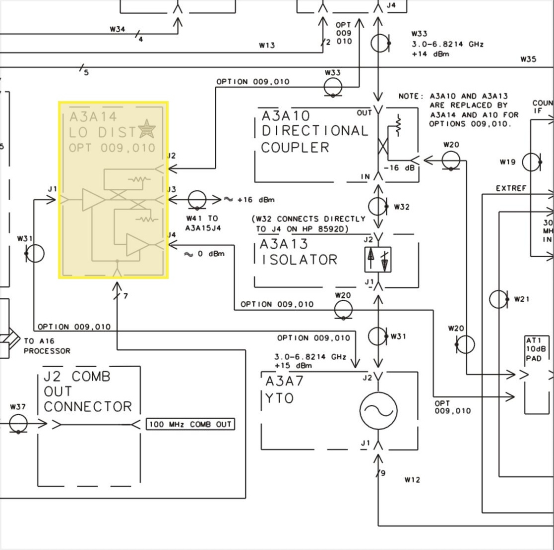
Bummer, half an hour later the working YTO is installed but the ERR 334 still remains. Damn, all the work "for the cat" as we tend to say in Germany. So let's switch to a more analytical approach and actually take some measurements. The most important tool to repair a spectrum analyzer is - of course - another spectrum analyzer, so let's check the output on the 1st LO SMA jack on the front of the instrument.
But first, let's do a proper YTO alignment as I swapped the oscillator following the "8560E service guide". This involves switching the jumper for the main YTO PLL control voltage on the A14 RF board from "normal" to "test". The manual describes a way to adjust the lower 3.20 GHz and upper 6.01 GHz setpoints for pretuning to center the YTO within the locking range of the PLL.
The output level on the 1st LO output on the unit's front panel should be in the range of +16 to +18 dBm but I measure approximately -15 dBm, this is way off! Hopefully I didn't kill the YTO while swapping it...
So lets measure the output power on the YTO itself by disconnecting the semirigid cable between the YTO and the LO distribution amplifier. Adding a 10dB attenuator on the YIG and measuring directly reveals +15 dBm which is perfect so the issue must be within the LODA. A quick check on the other outputs on the distribution amplifier shows the same behavior, the mixer output is around -15 dBm, too. The sampler output is at roughly -30 dBm, so 15dB below the mixer level, it should be around 0 dBm.
Another hint towards a defective LODA is that it's pulling down the +5V supply voltage to 4.6V and it is generating lots of heat. The negative gate bias voltage is at +300mV. Without the LODA connected, it sits a -600 mV as expected, so the LODA is pulling it up. Not a good sign!
Removing the LODA and testing it with a bench power supply leads to the same conclusion: It's more of an attenuator and space heater than an amplifier.
ATTENTION: RUNNING THE LODA WITHOUT APPLYING NEGATIVE BIAS TO THE GATE BIAS PIN WILL DESTROY THE MODULE !!!!
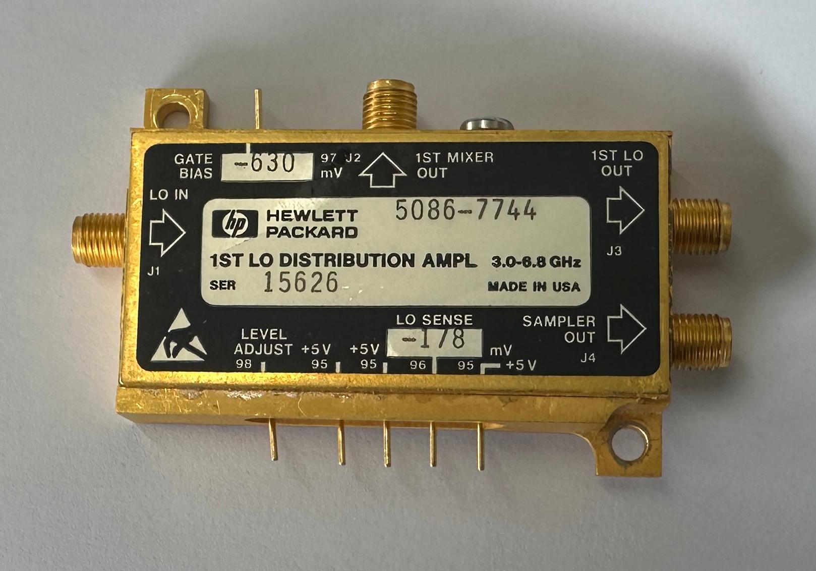
As it is already broken, let's crack open the lid which is held in place by conductive glue and let's try to get a clue on how the module works.
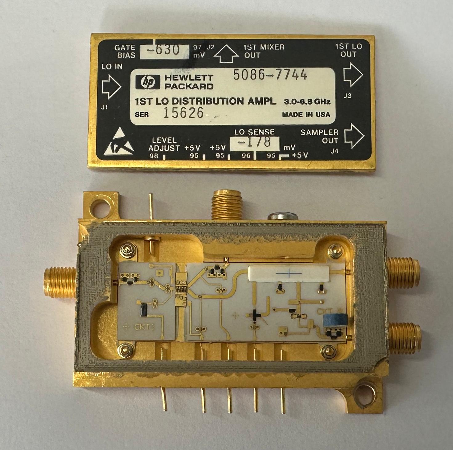
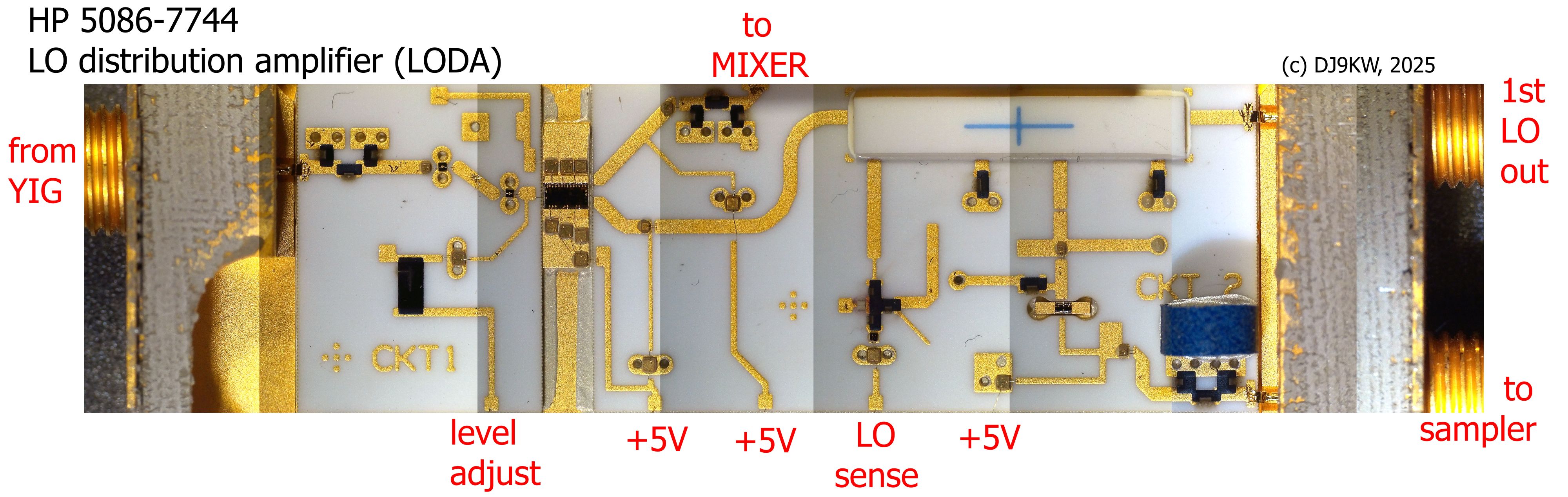
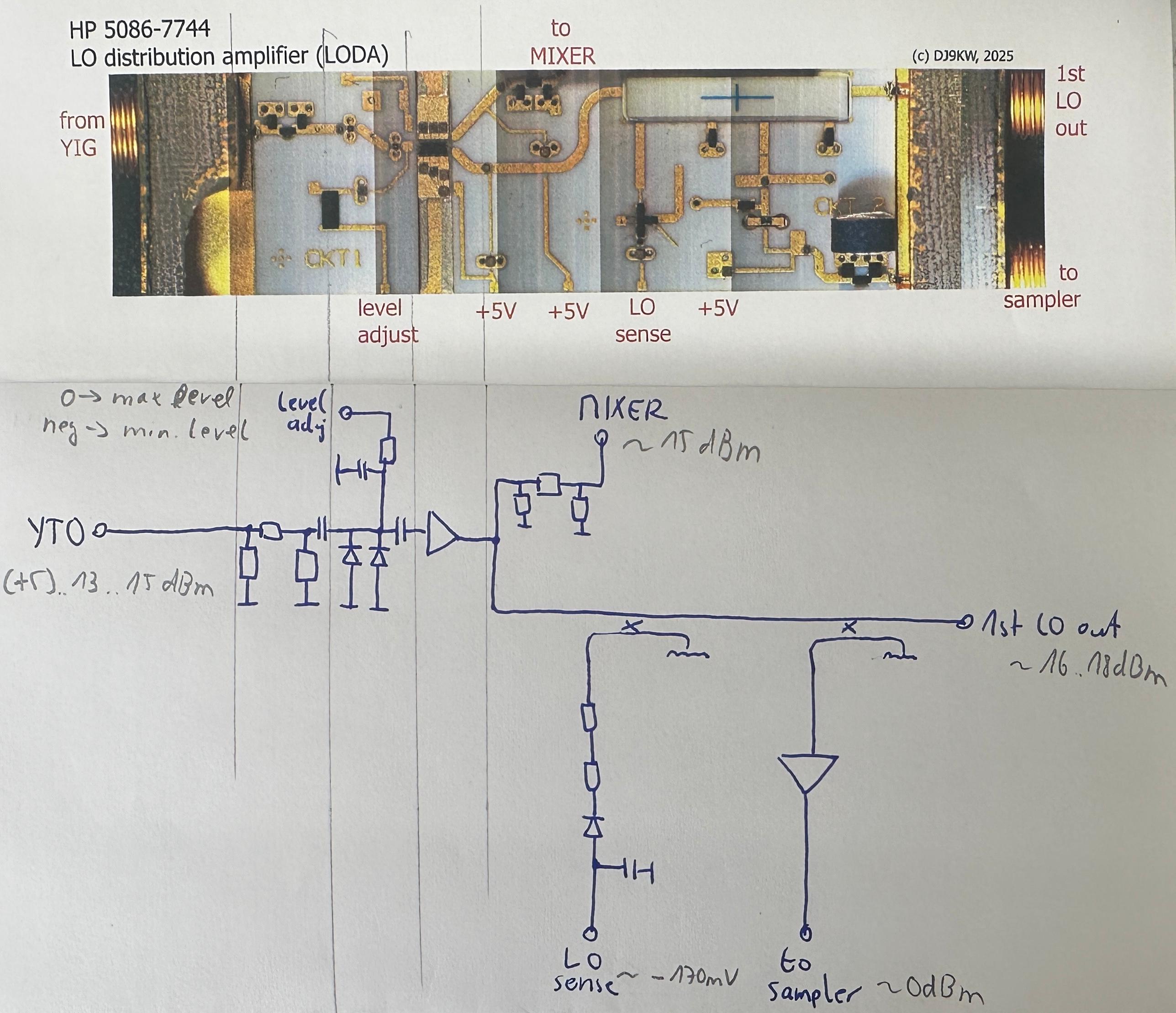
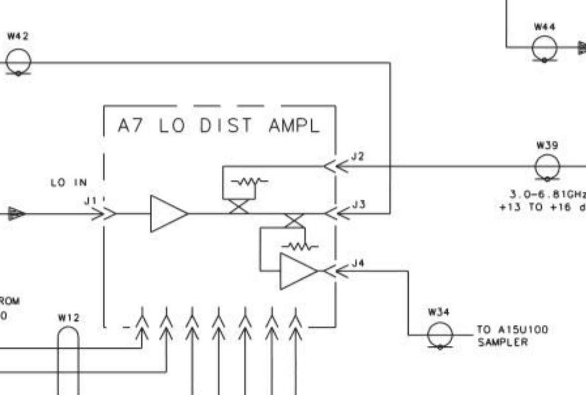
On the left side you can see the input from the YTO. According to the internet, the LODA requires an input level between +5 and +18 dBm to achieve a leveled output. A well behaving YTO should output around +13 to +15 dBm while a slightly tired one is just shy of +11 dBm, so still within the acceptable limits of the LODA (at least by now...).
The first element after the input is an attenuator for matching the YTO output. This is followed by an adjustable attenuator consisting of two paralleled PIN diodes which can shunt the signal to ground.
The bias resistor supplying the pin diodes, which is printed on the ceramic substrate, measures 700 ohms.
No voltage applied results in virtually no attenuation, the more negative the control voltage gets, the more attenuation is applied. What a weird design, I would have chosen to use the classic three PIN diode approach which at least tries to resemble a 50 Ohm load... This setup just pulls the rf signal to ground. But yeah, if it works...
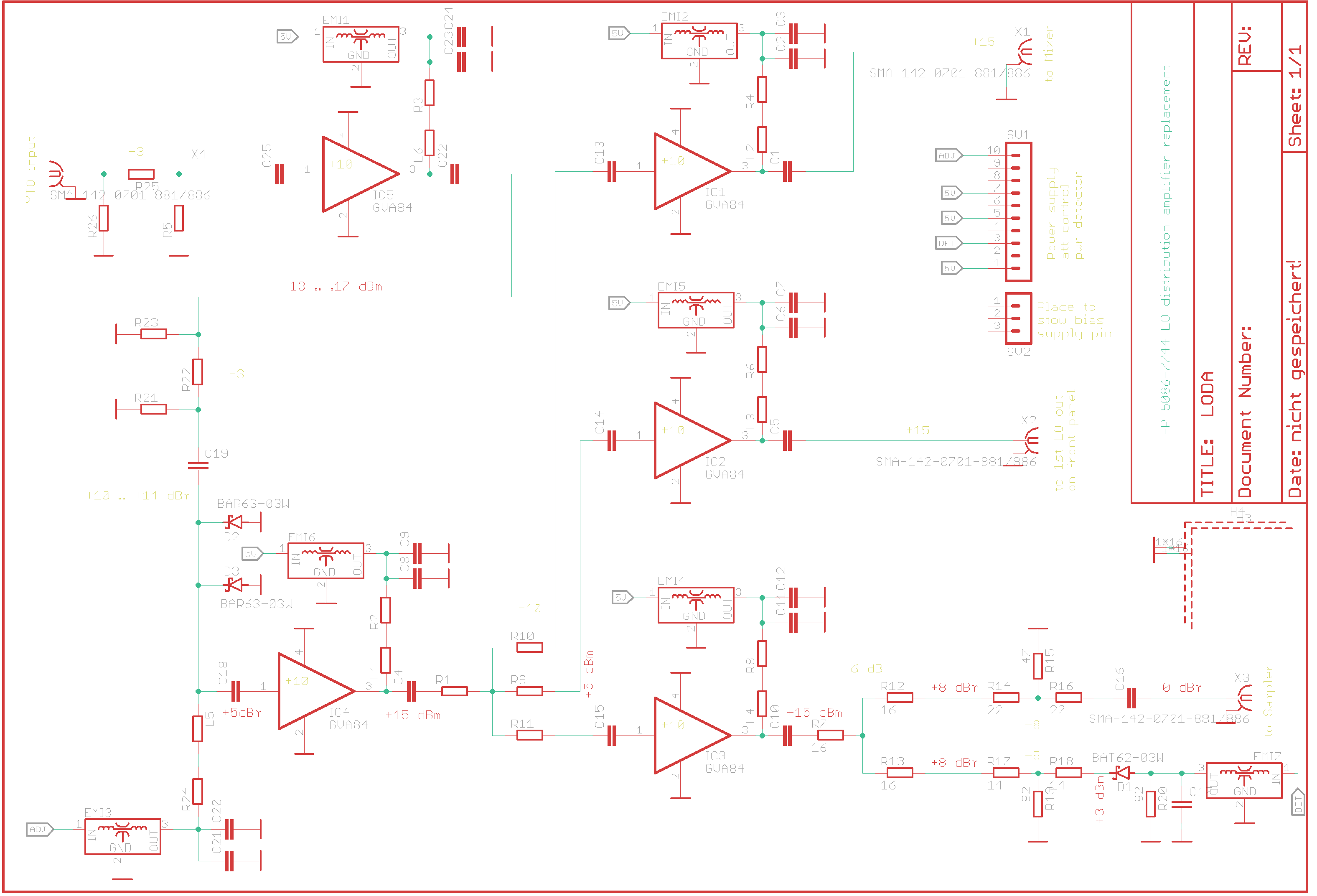
Looking at the block diagram from HP and the hybrid circuit, this seems to be the schematic of the module:
As with most HP stuff from this era, it's a beautiful piece of engineering but a nightmare when it comes to repairing these things!
Probably the main amplifier is dead and I don't see any easy way to fix this as a wire bonder isn't the most common tool and not available... So the only thing to do is looking for a donor LODA (and man, they are expensive! Prices for HP stuff are insane!) or going a different route and designing a replacement.
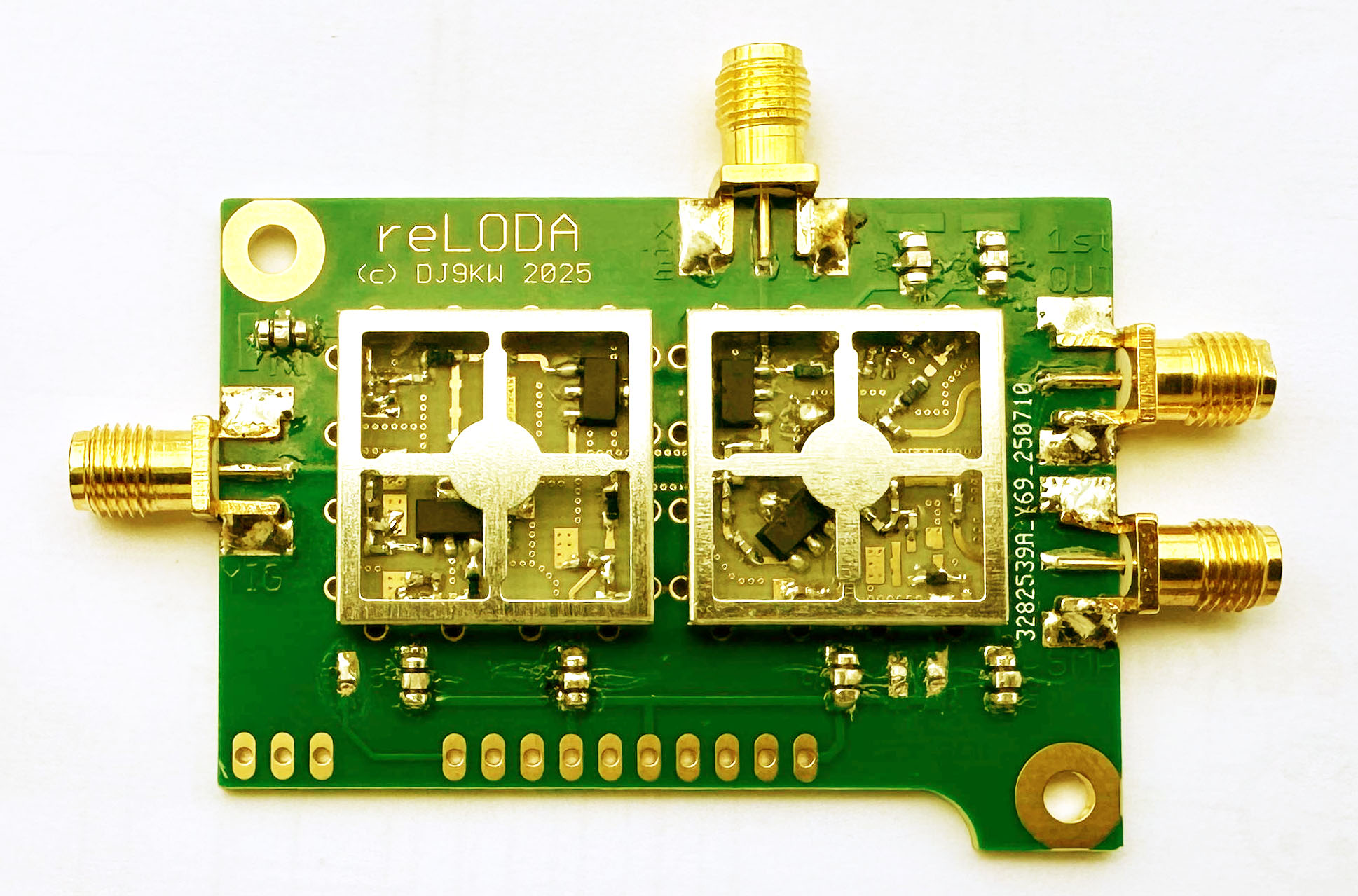
As PCBs and MMICs are rather cheap nowadays, that's the way to go!
A couple hours later I ended up with the following design, eagerly waiting for delivery from my go-to pcb manufacturer, JLC-PCB:
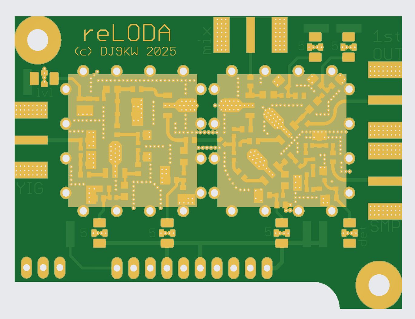
And fast forward several days, my experimental replacemenbt board arrives and I can start to populate all the parts (still one Mouser order away from completion... :)
(c) DJ9KW, 07/2025
PREV: HP chronicles overview
OVERVIEW
NEXT: HP YIG bonanza